What are the Characteristics of Diode?
What are the Characteristics of Diode?
Diode Definition
We use semiconductor materials (Si, Ge) to form variety of electronic devices. The most basic device is diode. Diode is a two terminal PN junction device. PN junction is formed by bringing a P type material in contact with N type material. When a P-type material is brought in contact with N- type material electrons and holes start recombining near the junction. This results in lack of charge carriers at the junction and thus the junction is called depletion region. When we apply voltage across the terminals of PN junction, we call it as diode. The picture below shows the symbol of PN junction diode.
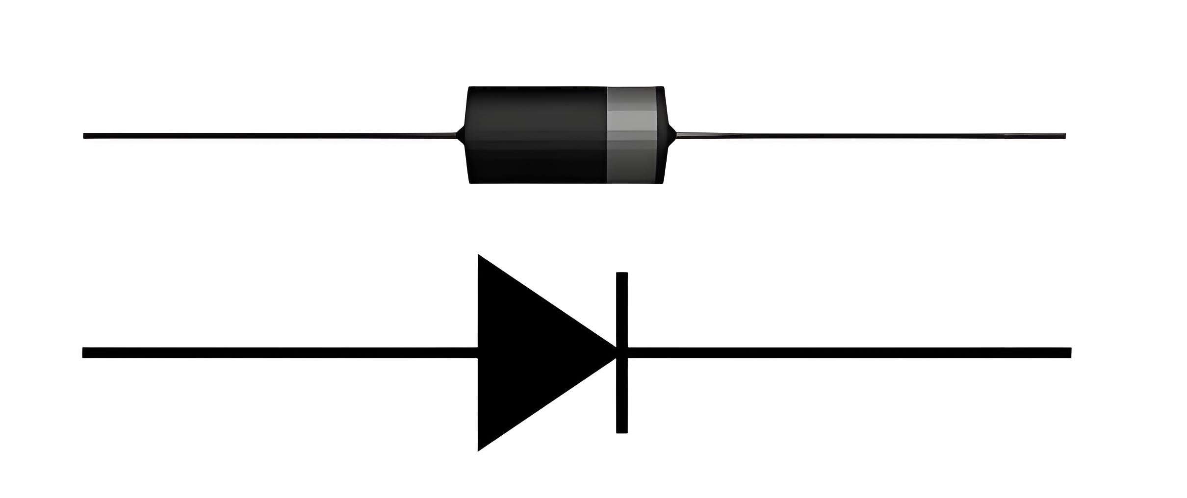
A diode is a unidirectional device that allows current to flow in only one direction, depending on how it is biased.

Forward Biasing
When the P-terminal is connected to the positive end of the battery and the N-terminal to the negative, the diode is forward biased.
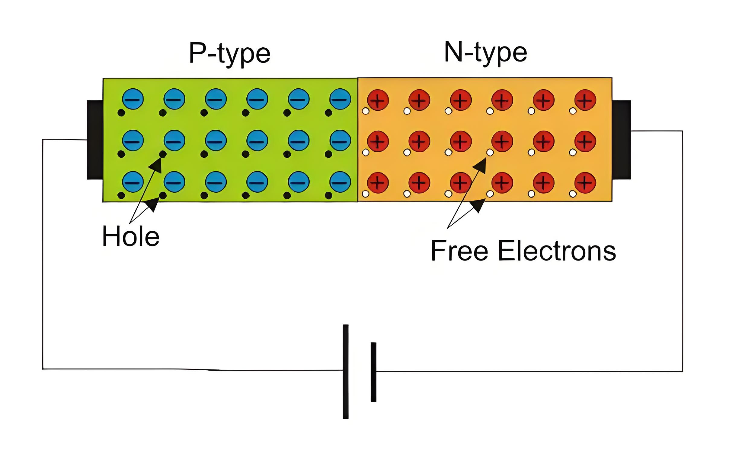
In forward bias, the positive battery terminal repels holes in the P-region and the negative terminal repels electrons in the N-region, pushing them toward the junction. This increases the concentration of charge carriers near the junction, causing recombination and reducing the width of the depletion region. As the forward bias voltage increases, the depletion region narrows further, and current rises exponentially.
Reverse Biasing
In reverse biasing P- terminal is connected to negative terminal of the battery and N- terminal to positive terminal of battery. Thus applied voltage makes N side more positive than P side.
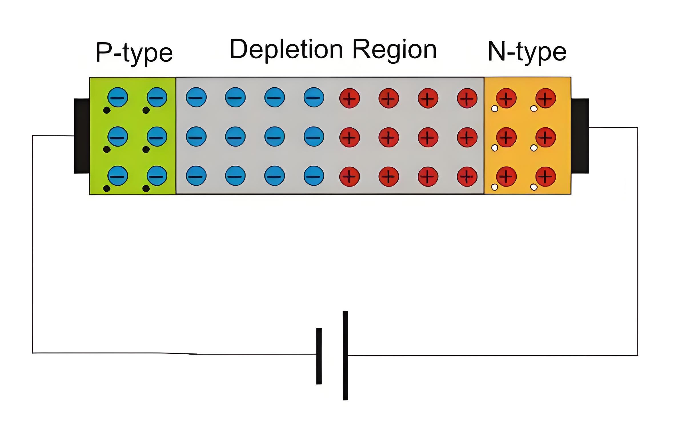
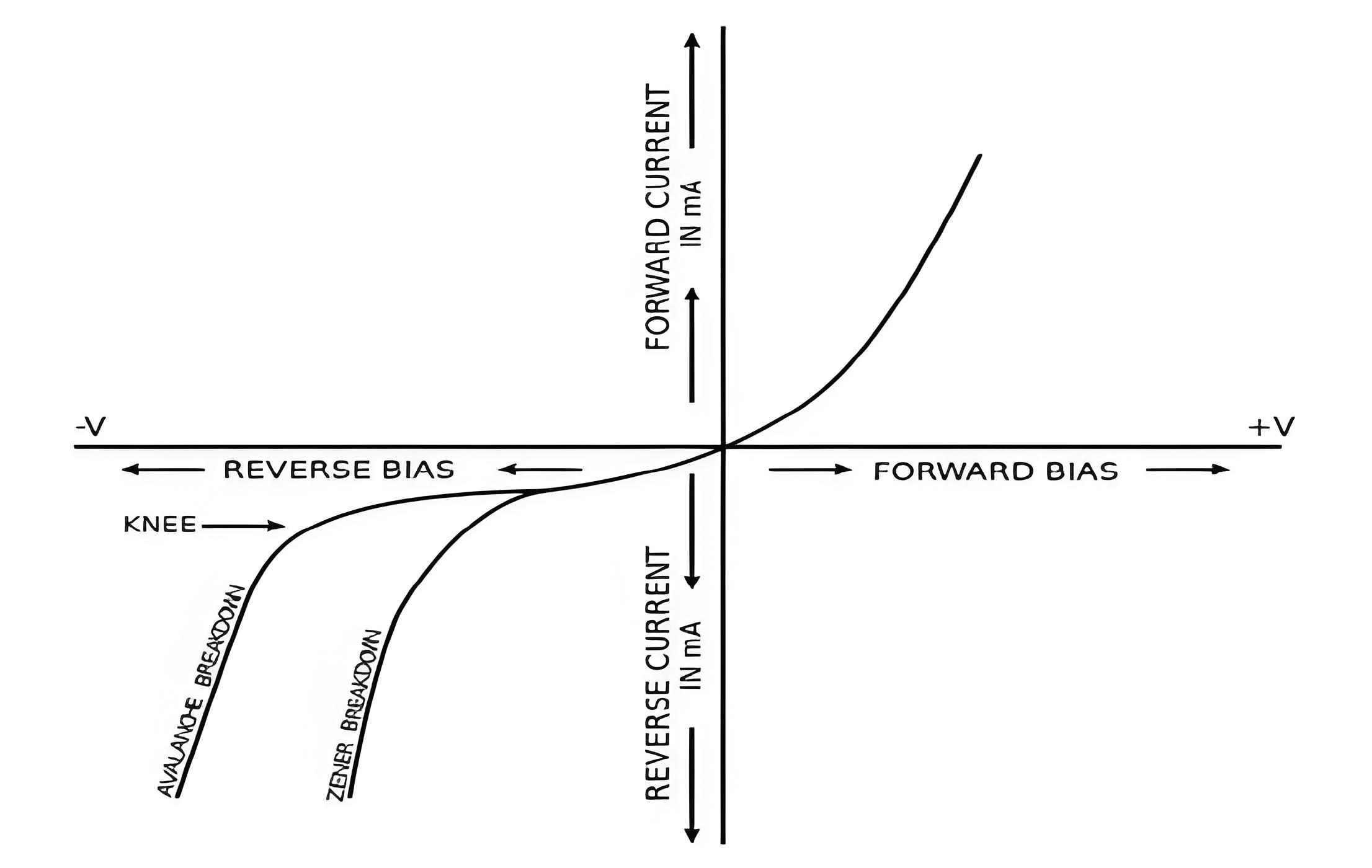
Negative terminal of the battery attracts majority carriers, holes, in P-region and positive terminal attracts electrons in the N-region and pull them away from the junction. This result in decrease in concentration of charge carriers near junction and width of depletion region increases. A small amount of current flow due to minority carriers, called as reverse bias current or leakage current. As reverse bias voltage is raised depletion region continues to increase in width and no current flows. It can be concluded that diode acts only when forward biased. Operation of diode can be summarized in form of I-V diode characteristics graph.
As reverse bias voltage is further raised, depletion region width increases and a point comes when junction breaks down. This results in large flow of current. Breakdown is the knee of diode characteristics curve. Junction breakdown takes place due to two phenomena.
Avalanche Breakdown
At high reverse voltages, avalanche breakdown happens when minority carriers gain enough energy to knock electrons from bonds, leading to a large current flow.
Zener Effect
The Zener effect occurs at lower reverse voltages, where a high electric field breaks covalent bonds, causing a sudden increase in current and junction breakdown.
Welcome to our electricity community! Established to facilitate the exchange and cooperation in the electricity industry and bridge professionals, enthusiasts, and related enterprises.


